It seems like everyone’s getting excited about innovations in printed electronics. To the layperson, printed electronics is a new and exciting technology. But to the engineer, printed electronics is a well-established practice that continues to advance. 
In its simplest form, printed electronics is the process of printing electrically functional inks or other materials on a substrate using industrial printing processes involving the layering of multiple ink layers. Today, the printed electronics field is focused on the process – the printing methods and ink materials –that meet requirements and specifications related to the properties of printed materials, economic and technical considerations, and requirements related to printed layers.
We’ve put together this guide to provide today’s engineering professionals with the resources and information they need to know about the continuously advancing field of printed electronics.
In this guide, you’ll find:
- The Printed Electronics Industry
- Printed Electronics Technologies
- Printed Electronics Materials
- Types of Printed Electronics
- Printed Electronics Standards
- Additional Printed Electronics Industry Resources and Associations
The Printed Electronics Industry
IDTechEx predicts that the market for printed, flexible, and organic electronics will reach $73.43 billion in 2027, a projected growth of more than $44 billion, from $29.28 billion in 2017. The majority of this market, according to IDTechEx, is comprised of OLEDs (organic light emitting diodes, a flat light-emitting technology) and conductive ink that’s used in a wide variety of applications. They also identify a few key areas of tremendous potential growth including stretchable electronics, logic and memory, and thin film sensors, three areas which are just emerging from the R&D phase.
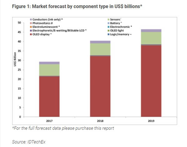
Screenshot via IDTechEx
In addition to OLED displays, two of the most successful applications for printed electronics to date include solar panels and glucose test strips, but in broader terms, many industries can benefit from printed electronics technology including:
- Consumer goods
- Healthcare
- Mobility
- Electronics
- Media
- Advertising
IDTechEx also points out the many benefits of these new and emerging technologies, including:
- Lower costs
- Improved performance
- Flexibility
- Transparency
- Reliability
- Improved environmental credentials
According to a report from MarketsandMarkets, another key driver of growth in printed electronics is the rapid penetration of the Internet of Things (IoT). According to the report, “Printed electronics, along with their low cost, provides added benefits of thin-form factor, flexibility, stretchability, portability, and rollability, among others. All these factors find an important application in wearable devices, smart packaging, healthcare, automotive, and other applications.”
Other sectors are rife for innovation with advanced printed electronics technologies such as 3D printing. Printed circuit boards (PCBs), for example, are one of the most common applications for printed electronics. As product manufacturers seek to shorten turnaround time for prototypes, there’s a clear need for faster and more cost-effective solutions. A 2016 survey of more than 300 electronics manufacturers and designers, The 3D PCB Printer Readiness Survey, conducted by Nano Dimensions Ltd., finds:
- 16% of respondents report that their companies spend more than $100,000 annually on PCB prototypes
- 17% spend between $50,000 and $100,000 annually
- 44% spend between $10,000 and $50,000 each year
- 23% spend less than $10,000 annually
Printed Electronics Technologies
Printed electronics promises lower costs as well as opportunities for innovative functionality, such as mechanical flexibility, that is traditionally more difficult (or impossible) and more expensive with conventional electronics approaches. Thanks to a variety of printed electronics technologies and printing methods, engineers have a variety of options for meeting project requirements and specifications.
Printing Methods
Printing methods include popular approaches such as inkjet printing and screen printing, both of which are well-suited for low-volume and high-precision projects. Printing methods include, but are not limited to:
- Inkjet printing – Flexible and versatile with low-effort setup, inkjet printing is suitable for low-viscosity, soluble materials such as organic semiconductors.

- Screen printing – Can produce thick, patterned layers using paste-like materials, making it suitable for producing conducting lines from inorganic materials such as antennas and circuit boards. Screen printing is also a useful method for insulating and passivating layers, particularly when the thickness of a layer is more important than resolution.
- Gravure – Formally, this printing method is called Rotogravure, although it’s often called Roto or Gravure. The process involves the engraving of an image onto an image carrier. It uses a rotary printing press to engrave images onto a cylinder.
- Offset printing – Offset printing is a legacy printing method that offsets, or transfers, an inked image from a plate to rubber sheet and then onto the printing surface.
- Flexographic printing – This printing technique makes use of a flexible relief plate. Similar to a letterpress, flexographic printing can be used on any type of substrate, from plastic, to metallic films, to paper.
- Aerosol Jet Printing – Also known as M3D (Maskless Mesoscale Materials Deposition), Aerosol Jet Printing begins by atomizing an ink, which produces droplets of one to two micrometers in diameter. These droplets are then delivered to a print head via a gas stream and impinge on the substrate at high velocity. This process enables the printing of conformal patterns on 3D substrates. The ink typically requires a post-treatment to achieve the desired electrical and mechanical properties.
- Evaporation printing – Uses a combination of high precision screen printing with material vaporization. Evaporation printing uses techniques such as thermal, e-beam, sputter, and others to deposit materials through a stencil (a high precision shadow mask) registered to the substrate. It allows for the layering of different mask designs using various materials.
Gravure, offset, and flexographic printing methods are more commonly used for high-volume production needs, such as solar cells. Offset and flexographic printing are primarily used for inorganic and organic conductors, while gravure printing is suitable for quality-sensitive layers thanks to its high layer quality as well as for inorganic and organic conductors for applications in which high resolution is required. Gravure printing may be used for organic semiconductors and semiconductor/dielectric-interfaces in transistors.
Printed Electronics Materials
Both organic and inorganic materials are used in printed electronics. When it comes to material selection, there are many options; the most suitable materials depend on the application requirements, costs, and other factors. Inks must function as conductors, semiconductors, dielectrics, or insulators and be available in liquid form.
Organic materials include conjugated polymers, which possess important characteristics such as conducting, semiconducting, electroluminescent, and photovoltaic properties. Other types of polymers may be used, but these are often used primarily as insulators and dielectrics.
Inorganic materials achieve some goals that organics and polymers can’t provide, such as highly ordered interfaces and layers. Both silver and gold nanoparticles may be used; silver is used with flexo, offset, and inkjet printing processes, while gold can be used with inkjet.
In general, there are several types of conductive inks commonly used for PE:
- Graphene Based Ink
- Circuit Scribe
- Nano-silver and nano- carbon inks
- Reactive Silver Inks
- Dielectric Inks
Engineers also have several options when it comes to substrates; again, the most suitable choice depends on the specific application requirements and objectives. Different printing methods are better suited for use with certain substrates, as well. For example, inkjet and screen printing methods are typically used with rigid substrates such as glass and silicon, but mass-printing methods are most often used with flexible substrates including foil and paper. Paper, however, is generally a problematic substrate for printed electronics applications for obvious reasons – not only is paper rough, but it’s also highly absorbent (although some innovations have successfully printed electronic components onto paper). Some flexible substrate options include:
- Poly(ethylene terephthalate)-foil (PET) – low cost with moderately high temperature stability
- Poly(ethylene naphthalate)- (PEN) – a higher-cost, higher-performance alternative
- Poly(imide)-foil (PI) – a higher-cost, higher-performance alternative
When it comes to substrates, the most important characteristics are smoothness and wettability. Some substrates can be prepped for better suitability using pre-treatments such as coating or Corona discharge. Highly-absorbent substrates such as paper are not typically suitable for printed electronics applications.
There are several important considerations when it comes to selecting the right conductive inks:
- What material is best-suited to your application?
- How conductive is your ink of choice? Does it require any pre-printing processes to increase conductivity?
- What substrates can your ink of choice be printed on?
- Is ink customization an option?
- What other costs are involved in the big picture? For instance, lower-conductivity inks often require the use of a greater volume of ink, so although an ink may be cheaper, it may cost the same or more than a higher-conductivity ink to achieve the same goals.
But it’s not just about choosing the right ink and the right printing technology. According to Dr. Gregory L. Whiting in an article for AZO Materials, “In addition to the properties of the printer itself, the substrate’s surface energy, solubility and roughness as well as the solutions’ surface tension, vapor pressure and solute chemistry all play important roles in controlling the resulting printed feature’s shape, position and structure. To reliably print electronic devices, these factors must all be carefully considered.”
Screenshots via AZO Materials
Printing Equipment
Of course, the development of innovative and hybrid printing methods has led to growth in printing equipment innovations, as well. The need to mass-produce printed electronics using desired inks and substrates at affordable costs has always – and will likely remain – a key driver of innovation. Some recent developments include both new takes on production machines as well as the development of new technologies and equipment for R&D purposes.
These needs have created opportunities for traditional printing equipment manufacturers to expand and innovate in new markets, and dozens of companies are getting in on the game including Xenon, AIXTRON, NovaCentrix, 3D-Micromac, Ceradrop, Adphos, and many others who are introducing tools for PVPD processes, photonic curing capabilities, modular roll-to-roll tools, and more.
Types of Printed Electronics
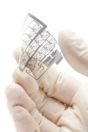
Because printed electronics is a growing and evolving field, specifying a definitive list of every printed electronics type is a challenging task. Printed electronics is having an influence on practically every facet of the broader electronics industry. Some examples of printed electronics applications include:
- Active-matrix backplanes, particularly for reflective displays
- Integrated circuits such as complementary invertors
- Antennas
- Ring oscillators
- Memory devices
- Printed organic and inorganic PV
- Light-emitting diodes
- Solar cells
- Various types of sensors such as RFID tags
- Batteries
- Wearables
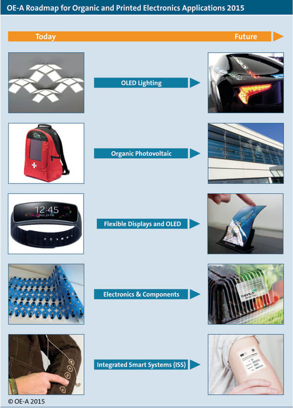
Screenshot via OE-A
Many of these types of electronics are printed as individual components which are then integrated into larger, more complex devices. That’s why PE is so prevalent; even devices that aren’t categorized as printed electronics may contain components that are. The proliferation of printed electronics has only just begun, and in the coming years, PE will continue to replace traditional electronics manufacturing processes with faster, more cost-effective innovations.
Printed Electronics Standards
As printed electronics is an evolving field, the development of industry-wide standards is also an ongoing process. There are several applicable standards and widely-accepted industry resources including:
- IEEE 1620-2004 – Standard for Test Methods for the Characterization of Organic Transistors and Materials. This standard covers recommended methods and standardized reporting practices for electrical characterization of organic transistors. It describes the most common sources of measurement error and recommends best practices to minimize and/or characterize the effect of each source.
- IEEE 1620.1-2006 – IEEE Standard for Test Methods for the Characterization of Organic Transistor-Based Ring Oscillators. This standard covers recommended methods and standardized reporting practices for electrical characterization of printed and organic ring oscillators. Like IEEE 1620-2004, the most common sources of measurement error are described along with best practices for avoiding, minimizing, and/or characterizing the effects of each source.
- IPC/JPCA-4921 – Requirements for Printed Electronics Base Materials. This standard provides data to aid in determining material capability and compatibility for flexible and rigid base dielectric materials for manufacture of printed electronics.
- IPC/JPCA-4591 – Requirements for Printed Electronics Functional Conductive Materials. This standard includes data to aid in determining material performance, capabilities, and compatibility of functional conductive materials for the manufacture of printed electronics.
- IPC/JPCA-2291 – Design Guideline for Printed Electronics. This standard is an overview of the design process flow for printed electronics based devices, modules and units, and final products.
- IPC/JPCA-6901 – Application Categories for Printed Electronics. This standard establishes a Market Classification System and Level Classification System for printed electronics assemblies. Additionally, it provides a list of performance criteria and testing methods, a standardized product category structure for designing printed electronics that conform with industry-accepted performance metrics.
- IPC-6903 – Terms and Definitions for the Design and Manufacture of Printed Electronics (Additive Circuitry). This standard includes industry-accepted terms and definitions in effort to create a common language for users and suppliers.
- ET-4101 – Printed Electronics – Materials – Part 1-1: Substrate (polymer and glass). Issued by JEITA, ET-4101 is focused on substrate materials, particularly polymer and glass.
- ET-4201 – Printed Electronics – Materials – Part 2-1: Ink of functional materials – Conductive material ink. Also issued by JEITA, ET-4201 focuses on functional materials, particularly conductive material ink.
- ET-4501 – Printed Electronics – OLED elements – Mechanical stress testing of OLED elements formed on flexible substrates. JEITA’s ET-4501 focuses on OLED elements, specifically mechanical stress testing of these elements formed on flexible substrates.
- TC 119 – TC 119 (the IEC’s Technical Committee leading standardization efforts related to printed electronics) focuses on the standardization of terminology, materials , processes, equipments, products and health/safety/environment in the field of printed electronics.
Other Standards Currently in Development
In addition to the IPC standards listed above, IPC has several additional standards in development including:
- IPC-4591A, Requirements for Printed Electronics Functional Conductive Materials
- IPC-4921A, Requirements for Printed Electronics Base Materials
- IPC-2292, Design Standard for Printed Electronics on Flexible Substrates
- IPC-6902, Qualification and Performance Specifications for Printed Electronics
Additional Printed Electronics Industry Resources and Associations
- International Electronics Manufacturing Initiative (iNEMI) – This organization publishes roadmaps on the global electronics industry as well as specific roadmaps pertaining to industry subsets. A robust collection of resources is valuable to any engineer navigating the evolving world of printed electronics.
- IPC—Association Connecting Electronics Industries – IPC has published several applicable standards (listed above). A global trade association that serves the printed board and electronics assembly industries, as well as their customers and suppliers, IPC is a well-respected authority in the industry. IPC’s standards are part of IPC’s Printed Electronics Initiative.
- The Organic Electronics Association (OE-A) – This organization is the leading international association for organic and printed electronics. OE-A also issues a roadmap for the industry, the OE-A Roadmap for Organic and Printed Electronics, currently in its 6th edition which was released in 2015. OE-A has also established a Working Group for Standardization/Quality Control and Measurement and a Working Group Encapsulation.
- International Electrotechnical Commission (IEC) – IEC is a global organization that publishes international standards and supports conformity assessment for devices that use or produce electricity, as well as those that contain electronics.
- SEMI – SEMI is the global industry association serving the manufacturing supply chain for the micro- and nano-electronics industries, including printed electronics, flexible electronics, and other micro- and nano-electronics-related industries.
- JEITA – The Japan Electronics and Information Technology Industries Association promotes healthy manufacturing, international trade and consumption of electronics products and components in order to contribute to the overall development of the electronics and information technology (IT) industries. JEITA has published several standards related to printed electronics, which can be found here.
- IDTechEx – While not exclusively dedicated to printed electronics, IDTechEx is an independent market research firm focused on emerging technologies, including printed electronics. In addition to market research, IDTechEx provides business intellligence and hosts a number of industry-relevant events. IDTechEx also runs Printed Electronics World, a digital publication offering the latest news and updates related to printed electronics.
- Printed Electronics Now – Another valuable online resource dedicated exclusively to reporting on the latest technologies and advancements impacting the field of printed electronics.